Custom Sim Racing Button Box
My first end-to-end PCB design, from schematic capture to routing.
Problem
Button boxes are essential peripherals in sim racing, enabling rapid access to controls and a more immersive workflow. Due to the niche market and low production volumes, commercially available options are limited. This gap motivated the decision to design and build a bespoke unit.
Goal
Deliver a reliable, configurable button box tailored to my sim racing setup.
Approach
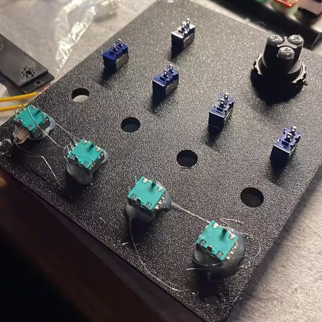
The Point-to-Point Era
The initial concept used discrete buttons with an Arduino Pro Micro, which was selected for native HID support. However, its limited I/O required a button matrix, and the wiring effort became excessive. Each switch and encoder needed individual soldering, plus diode isolation to prevent key ghosting. The prototype was therefore paused before assembly.
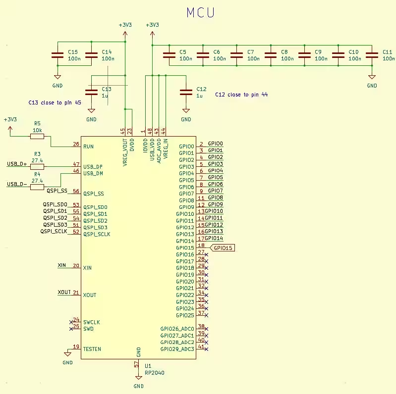
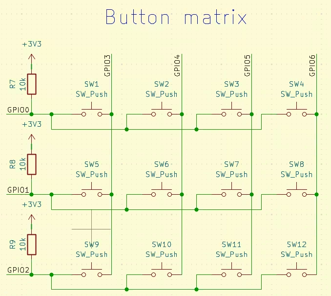
Schematic Capture
At that point, I committed to a dedicated PCB design. I already had foundational experience with KiCad from university projects, which made it a practical choice for schematic and layout work.
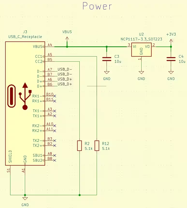
The first decision was the MCU. I selected the Raspberry RP2040 for its strong ecosystem and approachable development flow. Because fabrication was planned with JLCPCB, component selection and footprint validation were handled up front, followed by the schematic capture.
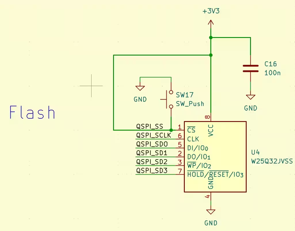
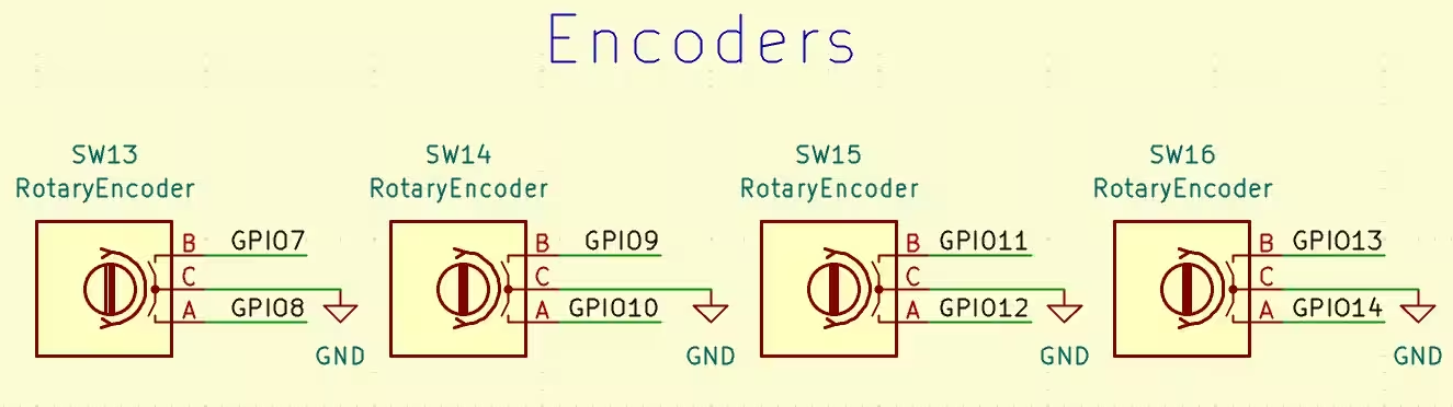
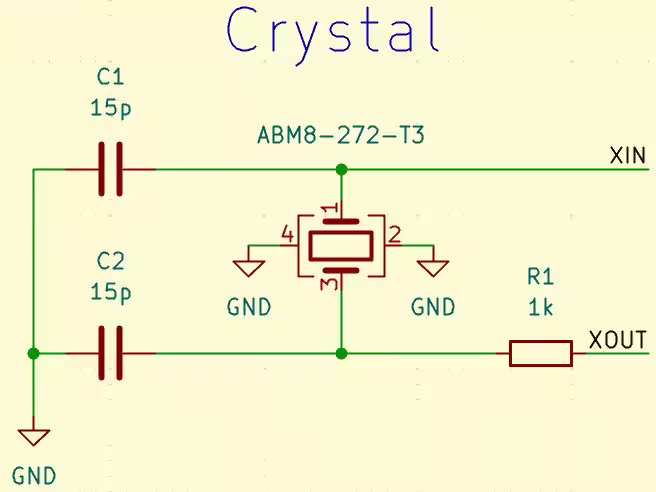
Building the schematic was the most demanding learning phase. Understanding component constraints and proper wiring required iteration, but the design stabilized into a coherent system.
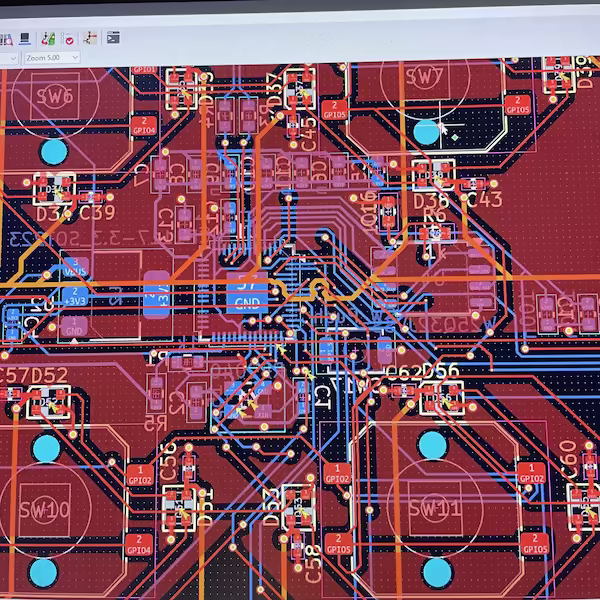
PCB Routing
Routing introduced a second major challenge. After several iterations of re-routing and reviewing best practices, the board reached a stable layout. The per-button and per-encoder LED plan increased routing complexity significantly, and I did not have access to a formal design review. The final layout reflects the best practices and constraints I could validate independently.
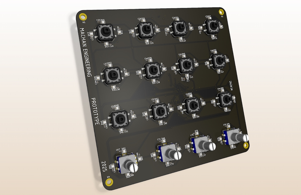
Final Design
A 3D render of the final design is shown below. The next step is fabrication. The remaining decision is whether to order an assembled PCB or a bare board for manual assembly.
Result
A completed button box PCB design ready for manufacturing.